SUMMARY
- The Union Government is in the process of preparing to initiate the second phase of the India Semiconductor Mission.
- The focus would be on enhancing the availability of raw materials within Semicon 2.0.
- The commencement of the second phase is anticipated to occur within three to four months.
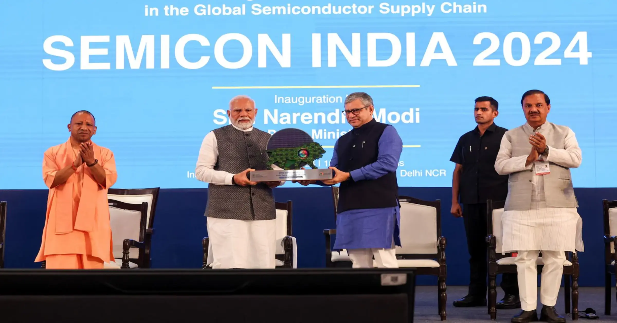
The Union Government is in the process of preparing to initiate the second phase of the India Semiconductor Mission, which will broaden its scope beyond semiconductor fabrication and chip packaging to include component companies, raw material suppliers, and other pivotal entities within the ecosystem, Electronics and Information Technology Minister Ashwini Vaishnaw has announced at the Semicon India industry conference in Greater Noida.
The commencement of the second phase is anticipated to occur within three to four months. The formulation of Semicon 2.0 is underway, aiming to create a more extensive version of the initial phase, with the objective of establishing the entire ecosystem.
Additionally, the government intends to focus on enhancing the availability of raw materials within Semicon 2.0. The Information Technology Ministry is set to present the Cabinet with several new proposals and a modernization plan for the Semiconductor Laboratory in Mohali in the near future.
Vaishnaw emphasized that the industry has already forged partnerships with academia, noting the necessity of 250 chemicals and gases for semiconductor production. He further stated that the emphasis will be placed on the development of the entire ecosystem, including equipment, specialized materials, and specialized gases and chemicals.
The expansion of the semiconductor industry in India, he mentioned, will further deepen this mission, positioning the country as a global leader in technology-driven solutions. Vaishnaw highlighted the swift progress achieved through the first phase of the Semiconductor Mission, noting the approval of five semiconductor units.
He stated that construction is in progress at Micron’s unit, and preparatory work has commenced on the Morigaon Tata unit, with additional projects scheduled to begin shortly. The record pace at which permissions are being secured has established a new global benchmark.
He added that 113 universities, academic institutions, and research organizations have integrated courses focused on semiconductor technology, in collaboration with industry leaders to ensure their relevance to real-world applications.
He further mentioned, “Programs such as LAM Research’s Semiverse, currently running across 74 universities, have trained over 2,600 students this year alone, with plans to scale massively in the coming years. Additionally, AMD’s global design center in Bengaluru has opened with 5,000 engineers, with further expansion on the horizon.”
The establishment of Applied Materials’ India Validation Center in Bengaluru, which will employ 200 engineers, is also slated to play a crucial role in supporting the development of fabrication facilities and Assembly, Test, Marking, and Packaging (ATMP) units in India, he added.
India’s existing expertise in semiconductor design is a key focus of the Semiconductor India Program, with over 300,000 engineers engaged in design roles across various companies, the minister mentioned.
“Of these, 52,000 engineers are engaged in leading-edge, complex chip designs,” Vaishnaw noted while discussing that 13 design ecosystem partners have received financial assistance through the semiconductor program, with four already attracting venture capital interest and two securing funding from venture capital firms.